Thursday, 14 March 2024

A Deep Dive on Digital Systems: Exploring Topics within the FE Electrical Exam Pt. 2

Welcome back to the topic of digital systems! We will continue where we left off and explore flip-flops and counters, programmable logic devices and gate arrays, state machine design, and timing (e.g., diagrams, asynchronous inputs, race conditions, and other hazards).
A Deep Dive on Digital Systems
Flip-flops and Counters
Flip-flops are edge-sensitive devices that are controlled by clock transitions. Their behavior and output depend on the rising or falling edges of the clock signal. Incorporating flip-flops into a circuit also adds state properties to the circuit, meaning the output relies not only on the current input of the system but also on its previous inputs.
A flip-flop is a sequential logic device. Thus, it has two possible output states: 0 or 1. Another contributing attribute to the output is that it is synchronized with a clock signal (CLK), ensuring that changes in the output should occur at specific clock time intervals. The signal Qn represents the value of the flip-flop's output before the application of the CLK signal, while Qn+1 represents the output value after the CLK signal has been applied. There are 3 basic flip-flops that you need to know for the FE exam: D flip-flop, SR flip-flop, and JK flip-flop.
1.D Flip Flop
D Flip FlopFigure 1
The master-slave flip-flop exhibits distinct characteristics in its operation. A change to the input, D, will affect the “Master D latch”, while the slave output shall remain unchanged. As the clock pulses back to 0, the master section will be disabled, isolating it from the D input; simultaneously, the slave section then becomes enabled.
This change in master influence allows the value of Y to be transferred to the flip-flop's output at Q. Notably, a change in the flip-flop's output can only be triggered during the transition of the clock from 1 to 0, providing precise timing control for the circuit's behavior (Widmer et al., 2017, 260-261).
The truth table for the D flip-flop is shown below: 

D

Qn+1


0

0

Reset

1

1

Set

The characteristic equation is depicted below
Qn+1 = D
2. SR Flip Flop
SR flip flop stands for Set Reset flip flop. SR flip-flop (Figure 2) is constructed with the use of a NAND latch and two NAND gates (Widmer et al., 2017, 256).
SR Flip Flop
Figure 2
The truth table for SR flip-flop is shown as below

S

R

Qn+1


0

0

Qn

No change

0

1

0

Reset

1

0

1

Set

1

1

Indeterminate

Indeterminate

The characteristic equation is depicted below:
Qn+1= S + QnR'
3. JK Flip Flop
The JK flip-flop can be seen as the improved iteration of a SR flip-flop; its design addresses the issue of an indeterminate state that arises when both inputs of the SR flip-flop are set to 1 (Widmer et al., 2017, 258).
In the JK flip-flop:
  • The J input functions similarly to the S input of the SR flip-flop, intended to set the flip-flop to a particular state.
  • The K input behaves akin to the R input of the SR flip-flop, responsible for resetting the flip-flop and changing its state (Widmer et al., 2017, 259).
The logic circuit of a JK flip-flop (Figure 3) is built by utilizing an SR flip-flop that is itself constructed from a NAND latch (Widmer et al., 2017, 259-260).
JK flip-flop
Figure 3
The truth table for JK flip-flop is shown as below: The characteristic equation is depicted below

J

K

Qn+1


0

0

Qn

No change

0

1

0

Reset

1

0

1

Set

1

1

Q'n

Compliment

The characteristic equation is depicted below:
Qn+1= JQ' + K'Q
Programmable Logic Devices and Gate Arrays
1. Programmable Logic Devices (PLD)
PLDs, also known as field-programmable logic devices (FPLDs), offer the flexibility to create a wide range of digital circuits, from simple logic gates to complex digital systems.
With the understanding that any function can be expressed in sum-of-product (SOP) form, a programmable logic device (PLD) is composed of the following components (Widmer et al., 2017, 948):
  • Input buffers and inverters generate both the original and complement forms of each input variable.
  • A set of AND gates, where the inputs can be programmed or selected.
  • A set of OR gates, where the inputs can also be programmed or selected.
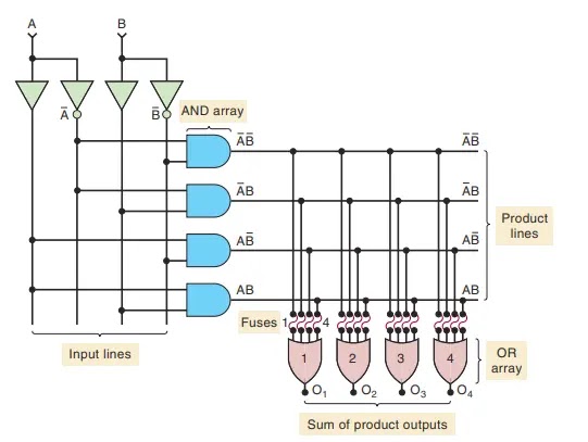
Programmable Logic Devices
Figure 4
Example:
Figure 5
Figure 5
Write the functions of f1 and f2 for the PLD above?
We just need to carefully examine which input and out are being connected to the gate.
f1 = x1x2 + x1x3' + x1'x2'x3
f2 = x1x2 + x1'x2'x3 + x1x3
2. Gate Arrays
Gate arrays are highly integrated circuits with a vast number of gates, often numbering in the hundreds of thousands. These devices rely on pre-fabricated gates that are interconnected to create the desired logic functions. The gate interconnections are determined by a custom-designed mask specific to the application, similar to the data stored in a mask-programmed read-only memory (ROM). Due to this characteristic, gate arrays are sometimes referred to as mask-programmed gate arrays (MPGAs) (Widmer et al., 2017, 943). While individually less expensive than PLDs with a similar gate count, gate arrays require custom programming, which adds complexity to their implementation.
State Machine Design
A state machine refers to a mathematical model or an abstract machine that exhibits different states and transitions between those states based on input conditions. It is a fundamental concept used to design and control sequential logic circuits.
A state machine consists of a finite set of states, a set of inputs, a set of outputs, and a set of transitions that define the behavior of the machine. The current state represents the internal condition of the machine, and the transitions determine how the machine moves from one state to another in response to input signals (Widmer et al., 2017, 481).
Let’s take a look at this flip flop circuit (Figure 6).
State Machine Design
Figure 6
To construct a state diagram of Figure 6, the following steps need to be followed:
  1. Obtain the function of the circuit: Understand the behavior and logic of the system to define its function.
  2. Determine the four main components: Identify the present state, inputs, next state, and output of the circuit. These components define the behavior and transitions within the system.
  3. Create a truth table: Combine the function and the four components to form a truth table. The truth table represents all possible combinations of inputs and current states, along with the corresponding outputs and next states.
  4. Obtain the binary result: Analyze the truth table to determine the binary representation of the system's behavior and transitions. This binary result serves as the foundation for constructing the state diagram.
The equation for this flip-flop is an XOR function, and the truth table is constructed below.
A (t+1) = A x y

Present state

Inputs

Next state

A

x

y

A

0

0

0

0

0

0

1

1

0

1

0

1

0

1

1

0

1

0

0

1

1

0

1

0

1

1

0

0

1

1

1

1

Figure 7

Figure 7

We see that this state machine uses a single flip-flop. Therefore, it has two distinct states. Looking at the state diagram (Figure 7), these two states are represented as two circles, and the arrows indicate which input combination allows the current state to change from one to the other. The number inside the circles indicates that both the present state and the output can be either 0 or 1. For each state, the two inputs can assume four potential combinations.
Timing
A timing diagram is a visual representation of a set of signals in the time domain, usually consisting of a clock signal and an input and output.
The use of timing diagrams helps to find and diagnose digital logic hazards: Static, Dynamic, and Function Hazards. Logic Hazards are undesirable effects caused by either a deficiency in the system or external influences on the system (University of Surrey, n.d.). This can occur when changes in the input variable(s) do not change the output correctly.
  1. Static Hazards are when one input variable changes the output changes momentarily.
  2. Dynamic Hazards are when an output changes more than once from a single input change.
  3. Function Hazards are when more than one input variables change at the same time.
Conclusion
Through this two-part blog series, I have offered concise explanations for each digital systems topic found on the FE Electrical exam. If you are looking for more comprehensive exam prep, check out School of PE’s FE Electrical exam review course!
References
Widmer, N. S., Tocci, R. J., & Moss, G. L. (2017). Digital Systems: Principles and Applications. Pearson.
About the Author: Khoa Tran

Khoa Tran is an electrical engineer working at the Los Angeles Department of Water and Power and is currently pursuing his master's in electrical Power from the University of Southern California. He is fluent in both Vietnamese and English and is interested in outdoor activities and exploring new things.

Thursday, 7 March 2024

A Deep Dive on Digital Systems: Exploring Topics within the FE Electrical Exam

For those looking to take the Fundamentals of Engineering (FE) Electrical Engineering (EE) Exam we will delve into various concepts and components of digital systems. The topics can be found on this link.They include:
  1. Number systems
  2. Boolean logic
  3. Logic gates and circuits
  4. Logic minimization (e.g., Sum of Product (SOP), Product of Sum (POS), Karnaugh maps)
  5. Flip-flops and counters
  6. Programmable logic devices and gate arrays
  7. State machine design
  8. Timing (e.g., diagrams, asynchronous inputs, race conditions, and other hazards)
Please note that while we aim to cover a wide range of information, we have limited space and time. Therefore, we encourage you to explore further resources if you wish to delve deeper into any particular topic.
A Deep Dive on Digital Systems: Exploring Topics within the FE Electrical Exam
Number System
The number system refers to the different ways in which numerical values can be represented and manipulated. This is done to simplify and compress large numerical values into a few easily interpreted digits. Digital systems rely on these number systems: decimal system, binary system, hexadecimal system, and octal system.
  1. Decimal System
    The decimal system consists of a set of 10 symbols or numerals, namely 0, 1, 2, 3, 4, 5, 6, 7, 8, and 9. By utilizing these symbols as the digits of a number, we can represent any quantity within the decimal system (Widmer et al., 2017, 19).
  2. Binary System
    In the binary system, we only have 0 and 1, and each binary digit has its own value expressed as a power of 2 (Widmer et al., 2017, 21). The concept is depicted in Figure 1, where positions to the left of the binary point, analogous to the decimal point, represent positive powers of 2, while positions to the right represent negative powers of 2.
    Binary System
    Figure 1
  3. Hexadecimal System
    Hexadecimal is a numbering system represented in base 16, utilizing both numbers "0-9" and the alphabet "A-F" for double digit values "10-15".
  4. Octal System
    This numerical system is a base-8 system, using digits "0-7"
Boolean Logic
Boolean logic, named after mathematician and logician George Boole, is a fundamental concept in digital systems and computer science. It is a branch of mathematics and logic that deals with variables and operations based on the principles of true and false, or 1 and 0, respectively. Boolean algebra, unlike other mathematical systems, does not involve fractions, decimals, negative numbers, square roots, cube roots, logarithms, imaginary numbers, and similar mathematical concepts (Widmer et al., 2017, 71). Table 1 shows the common logic terms for the 0 and 1.

Logic  0

Logic 1

False

True

Off

On

Low

High

No

Yes

Open switch

Closed switch


Logic Gates
The three basic operations are NOT, AND (*), and OR (+). Below, you will find the definition, logic symbol, and corresponding Boolean expression for each function.
1. NOT Operation
NOT Operation
Figure x
The NOT operator or inverter (Figure x) inverts the sense of a binary value (0→1, 1→0) . It can be referred to as inversion or complementation. The NOT operation can be expressed as (Widmer et al., 2017, 80):
x = A or x = A'
The truth table is depicted below.

A

x

0

1

1

0

2. AND Operation
AND Operation
Figure x1
To illustrate the application of AND logic, let's take the example of a standard clothes dryer. The dryer will perform the drying process, including heating and tumbling, only if two conditions are met simultaneously: the timer is set above zero AND the door is closed. The AND circuit is illustrated in Figure x1. The AND operation can be expressed as (Widmer et al., 2017, 77-78):

x = A . B

The truth table is depicted below. 

A

B

x = A . B

0

0

0

0

1

0

1

0

0

1

1

1

3. OR Operation
OR Operation
Figure x2
Let's consider an example in a kitchen oven. The scenario involves the oven's light, which should be activated under two conditions: either the oven light switch is in the "on" position OR the oven door is opened. To represent these conditions, we can use variables A to denote the state of the oven light switch (true or false) and B to represent the state of the oven door (true or false). The variable x can then represent the state of the light (true or false). The AND circuit is illustrated in Figure x2. The OR operation can be expressed as(Widmer et al., 2017, 73-74):

x = A + B

The truth table is depicted below. 

A

B

x = A + B

0

0

0

0

1

1

1

0

1

1

1

1


Logic Minimization
Logic minimization refers to the process of simplifying and optimizing logical expressions or equations. It involves reducing the complexity of logical functions by eliminating redundancies and minimizing the number of logic gates required to implement the function.
There are two simplifications we will explore: sum-of-products (SOP) and product-of-sums (POS).
1. Sum-of-Products

SOP consists of two or more AND terms that are ORed together. SOP can also be referred to as Minterm. The function used to denote the sum of minterms is expressed below (Widmer et al., 2017, 138).

 f (x,y,z) =∑ m(h,i,j,..) = mh + mi + mj +...

The SOP is selected by f (x ,y ,z) = 1

2. Product-of-Sums

POS consists of two or more OR terms that are ANDed together. POS can also be referred to as Maxterm. The function used to denote the product of maxterms is expressed below (Widmer et al., 2017, 139).

 F (x ,y ,z) = ∏ M(h,i,j,...) = Mh . Mi . Mj

            The POS is selected by F (x ,y ,z) = 0

Given the truth table below, the expression of the SOP-Minterms and POS-Maxterms for the three binary variables can be obtained.

A

B

C

Minterms

Maxterms

Term

Designation

Term

Designation

0

0

0

A'B'C'

m0

A+B+C

M0

0

0

1

A'B'C

m1

A+B+C'

M1

0

1

0

A'BC'

m2

A+B'+C'

M2

0

1

1

A'BC

m3

A+B'+C'

M3

1

0

0

AB'C'

m4

A'+B+C

M4

1

0

1

AB'C

m5

A'+B+C'

M5

1

1

0

ABC'

m6

A'+B'+C

M6

1

1

1

ABC

m7

A'+B'+C

M7


Example: Find the expression for the function f as (a) sum of minterms and (b) product of maxterms using the following truth table.

A

B

C f

0

0

0

0

0

0

1

1

0

1

0

0

0

1

1

0

1

0

0

1

1

0

1

0

1

1

0

0

1

1

1

1


a) By following the rule of SOP, the sum of minterms can be obtained
f = A'B'C + AB'C' + ABC = m1 + m4 + m7
b) By following the rule of POS, the product of maxterms can be obtained
f = (A+B+C)(A+B'+C)(A+B'+C')(A'+B+C')(A'+B'+C) = M0 M2 M3 M5 M6
3. Karnaugh Map
A Karnaugh map consists of a grid-like structure, with input variables represented along the axes. Each cell in the grid corresponds to a specific combination of input variable values. The cells are typically labeled with binary values or decimal numbers, depending on the complexity of the function.
To simplify a logical function using a Karnaugh map, adjacent cells with 1s are identified and grouped together. These groupings, known as minterms, represent areas of the map where the logical function evaluates to true (1). By combining adjacent cells, redundant terms and logic gates can be eliminated, resulting in a simplified expression (Widmer et al., 2017, 152). Below are the steps on how to use Karnaugh maps or K-map to simplify logic expression (Widmer et al., 2017, 157-158).
a. Create a table
● In the FE Reference Handbook, you can find the K-map format in page xx to set up the table.

K-map-for-3-variables
Figure x: K-map for 3 variables

K-map-for-4-variables
Figure x: K-map for 4 variables

b. Complete the K-map from the truth table
● Place ‘0’ or ‘1’ into the corresponding cell term

A

B

C

f

0

0

0

1

0

0

1

1

0

1

0

1

0

1

1

0

1

0

0

0

1

0

1

0

1

1

0

1

1

1

1

0

K-map
Figure x
c. Form group of 1s
● Identify the 1s that are adjacent to only one other 1. Loop any pair containing such a 1.
● Groups can wrap around the edges and corners of the K-map.
● The “1” cells must be loop in an even group (groups of two, group of four, or group of eight). Make sure to use the minimum number of loops.
d. Form the Boolean expression
○ Each group represents the SOP equation.
Form the Boolean expression
f = A'B + BC'
The red group shares A = 0 and B = 0.
The blue group shares B = 1 and C = 0
e. The “Don’t Care”
○ “Don’t Care” is illustrated as an X in the truth table. It can be used as a ‘0’ or a ‘1’, whatever makes the looping easier.
Don’t Care
f = A' + C'D + BD
Conclusion Part 1
This is a lot of information to sort through on your first reading; please take the time to reread and practice problems on your own. We will finish the other half of these topics in an upcoming blog. Again, as this is only an introduction to these topics, it is highly encouraged that examinees explore School of PE’s FE Electrical exam review course to complement their exam prep.
References
Widmer, N. S., Tocci, R. J., & Moss, G. L. (2017). Digital Systems: Principles and Applications. Pearson.
About the Author: Khoa Tran

Khoa Tran is an electrical engineer working at the Los Angeles Department of Water and Power and is currently pursuing his master's in electrical Power from the University of Southern California. He is fluent in both Vietnamese and English and is interested in outdoor activities and exploring new things.